Executive Summary
The landscape of advanced materials science is undergoing a profound transformation, driven by the emergence of two-dimensional (2D) materials beyond the foundational graphene. This report delves into the unique properties and diverse applications of phosphorene, borophene, and MXenes, highlighting their potential to revolutionize various technological sectors. While graphene introduced the concept of atomically thin materials with exceptional properties, its inherent lack of a bandgap presented limitations for digital electronics. The subsequent exploration of phosphorene, borophene, and MXenes has unveiled a spectrum of electronic, optical, mechanical, and chemical characteristics that overcome graphene’s constraints and unlock novel functionalities.
career-path—enterprise-architect By Uplatz
Phosphorene, derived from black phosphorus, distinguishes itself with a tunable, direct bandgap and intrinsic anisotropic properties, making it highly promising for high-performance electronics and optoelectronics. Borophene, a metallic allotrope of boron, exhibits a remarkable versatility, capable of displaying both metallic and semiconducting behaviors, alongside potential for superconductivity, positioning it for advanced energy storage and biomedical applications. MXenes, a diverse family of transition metal carbides and nitrides, are characterized by outstanding metallic conductivity and highly customizable surface chemistries, making them ideal for multifunctional applications in energy storage, advanced sensing, and particularly, biomedicine.
Despite their immense promise, the widespread adoption of these next-generation 2D materials faces significant challenges related to scalable, consistent, and cost-effective synthesis, as well as long-term stability and integration into existing manufacturing processes. In this context, Artificial Intelligence (AI) is emerging as a transformative force, fundamentally reshaping the speed, scope, and methodology of materials discovery. AI accelerates data analysis, generates novel hypotheses, and automates experimental design through technologies like “self-driving labs,” significantly reducing the time and resources required for material development. However, the integration of AI also necessitates careful consideration of data quality, interpretability, ethical implications, and the crucial role of human oversight to ensure responsible innovation. The symbiotic relationship between these advanced 2D materials and AI is poised to drive the next wave of scientific breakthroughs and technological advancements across diverse sectors, from sustainable energy to advanced healthcare.
1. Introduction: The Evolving Landscape of 2D Materials
1.1 Defining 2D Materials and Their Fundamental Characteristics
Two-dimensional (2D) materials represent a groundbreaking class of substances, defined by their atomically thin nature, typically ranging from a single atomic layer to a few nanometers in thickness.1 This extreme dimensionality leads to a dramatic departure from the properties observed in their bulk counterparts, offering unique functionalities that are highly sought after in advanced technological applications.
A cornerstone characteristic of 2D materials is the phenomenon of quantum confinement. In these ultrathin structures, electrons are confined to a single dimension, akin to quantum wells, which fundamentally alters their energy levels from continuous bands to discrete states.1 This quantum mechanical effect is not merely a theoretical curiosity; it directly underpins the dramatic changes observed in the electrical, optical, and mechanical behavior of these materials, enabling a level of precision in material design previously unattainable. The ability to control energy levels at the nanoscale allows for the targeted engineering of specific functionalities, moving beyond serendipitous discovery towards a more deliberate design of materials.
Another critical attribute is their high surface-to-volume ratio.2 This expansive active surface area provides abundant sites for interaction with other molecules or environments, making 2D materials exceptionally efficient for applications such as gas sensing, catalysis, and energy storage. The increased surface area means more reactive sites are available for chemical reactions or charge adsorption, leading to enhanced performance in these domains.
Furthermore, 2D materials exhibit remarkably tunable properties.1 Their electronic band structures can span the full spectrum from metallic to semiconducting to insulating. The bandgap, a critical parameter for electronic and optoelectronic devices, along with carrier mobility, can be precisely modulated by adjusting the material’s thickness, applying mechanical strain, introducing an electric field, or altering its chemical composition. This inherent tunability provides a distinct advantage over traditional materials, allowing for bespoke material characteristics tailored to specific application requirements.
Mechanically, 2D materials possess exceptional strength and flexibility.1 Their strong in-plane covalent bonding results in high Young’s moduli and breaking strengths, making them suitable for robust yet flexible electronics and as reinforcement in composites. This mechanical resilience, combined with their thinness, enables the development of devices that can withstand significant deformation without fracture.
Finally, 2D materials display unique optical properties.1 These arise from the interplay of quantum confinement and reduced screening effects. They exhibit strong light absorption, photoluminescence (light emission), and distinct Raman scattering signatures. Crucially, their optical properties are often thickness-dependent, opening avenues for applications in photodetectors, light-emitting diodes (LEDs), and lasers, where precise control over light-matter interaction is paramount.
1.2 Graphene: The Foundational Material and Its Inherent Limitations
The field of 2D materials was fundamentally established with the isolation of graphene in 2004, a single layer of carbon atoms arranged in a hexagonal honeycomb lattice.1 Graphene quickly became the archetype for 2D materials due to its extraordinary combination of properties. It boasts exceptionally high carrier mobility, exceeding 200,000 cm²/V·s under ideal conditions, making it an unparalleled electrical conductor.1 Mechanically, it is approximately 200 times stronger than steel, yet remarkably flexible.11 Its thermal conductivity is also exceptionally high, reaching up to 5000 W/m·K, and it exhibits high optical transparency.1
Despite these “super material” attributes 13, graphene faces significant
inherent limitations for electronic applications, particularly in the realm of digital electronics. The primary challenge stems from its lack of a bandgap.11 As a perfect conductor, graphene cannot be easily “switched off,” which is a fundamental requirement for transistors and other digital logic devices that rely on distinct “on” and “off” states. While methods exist to engineer a bandgap into graphene, such as forming nanoribbons or applying electric fields, these often come at the cost of significantly reducing its vaunted electron mobility, bringing it down to levels comparable to strained silicon films.11 This presents a paradox: a material with unparalleled conductivity is limited in the very field where conductivity is paramount, due to its inability to switch. This fundamental electronic characteristic has been a primary driver for the exploration of other 2D materials.
Beyond its electronic limitations, graphene also faces considerable production and integration challenges. Current synthesis methods, including mechanical exfoliation and chemical vapor deposition (CVD), struggle to produce high-quality graphene in large quantities.12 This limited production volume restricts its availability and contributes to high costs, making it economically unfeasible for many widespread applications.12 Furthermore, existing techniques often lack the precision needed to ensure material consistency, leading to variations in size, defect density, and the number of layers, which directly impacts reliable performance and integration into devices.12
The handling of graphene also presents difficulties. Its single-atom thickness makes it prone to agglomeration and instability, complicating its manipulation during manufacturing processes and integration into existing workflows, often requiring new infrastructure and adaptations.12 Moreover, the absence of standardized production and quality control measures for graphene hinders its widespread adoption and trust within industries. Concurrently, ongoing investigations into the long-term health and environmental impacts of graphene necessitate further research and clear safety regulations for its responsible use.12 The market demand for specific electronic functionalities, rather than just extreme properties, is therefore a primary force pushing research into a broader array of 2D materials, emphasizing the need for materials with tailored electronic structures, particularly those with tunable bandgaps or semiconducting behavior.
2. Phosphorene: Properties, Synthesis, and Emerging Applications
2.1 Unique Structural and Anisotropic Electronic Properties
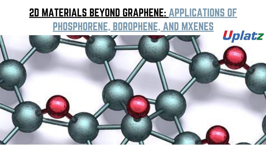
Phosphorene, the single- or few-layer form of black phosphorus, has emerged as a compelling 2D material, distinguished by its unique puckered honeycomb structure.1 This distinctive atomic arrangement is the direct cause of its intrinsic
anisotropic properties, meaning its characteristics vary significantly depending on the direction of measurement. This anisotropy is observed across its electronic, transport, optoelectronic, thermoelectric, and mechanical behaviors.1
In terms of electrical anisotropy, phosphorene exhibits significantly higher carrier mobility along its “armchair” direction compared to its “zigzag” direction.18 This direction-dependent conductivity makes it highly attractive for designing advanced electronic devices where current flow can be precisely controlled along specific pathways. Similarly, its
thermal conductivity is anisotropic, generally higher along the zigzag direction at room temperature, a property that can be leveraged in thermoelectric applications.18 Mechanically, its
Young’s Modulus also varies with direction, being high in the armchair direction and low in the zigzag direction.18 This directional strength and flexibility open up new avenues for device engineering, allowing for functionalities impossible with isotropic materials.
A crucial advantage phosphorene holds over graphene is its thickness-dependent direct bandgap, which ranges from approximately 0.3 eV in bulk black phosphorus to about 2 eV in its monolayer form.1 This tunable bandgap is fundamental for its application in high-performance electronics and optoelectronics, as it allows for precise control over light-matter interaction and charge carrier behavior, essential for device functionality. The presence and tunability of a bandgap directly enable applications in these fields that are challenging for graphene.
Phosphorene also boasts high electron and hole mobility, suggesting its potential to outperform other 2D semiconductors. This superior mobility is attributed to its lighter effective mass and narrower bandgap compared to some alternatives.17 However, a significant challenge for phosphorene is its
environmental instability.15 It is prone to rapid degradation when exposed to ambient conditions, specifically air and water, due to its reaction with oxygen and moisture, leading to the formation of phosphorus oxides. This susceptibility to degradation is a critical hurdle for its practical application and necessitates robust protection strategies.
2.2 Synthesis Methodologies and Stability Considerations
The fabrication of phosphorene is often described as “facile” 16, indicating a relative ease in its initial laboratory-scale preparation. Two primary approaches are employed for its synthesis:
Top-Down Methods involve exfoliating bulk black phosphorus crystals into single or few-layer phosphorene sheets, typically through mechanical exfoliation.15 This method, while straightforward, often yields small quantities and can introduce defects.
Bottom-Up Methods aim to synthesize phosphorene directly from atomic precursors. Hydrothermal synthesis, for instance, can provide a suitable environment for growing stable phosphorene, though it strictly requires oxygen-free conditions to prevent degradation.15 More advanced techniques like Chemical Vapor Deposition (CVD) and Molecular Beam Epitaxy (MBE) are actively being explored to achieve large-scale production with better quality control.18
Despite the “facile” nature of some synthesis routes, a significant challenge lies in the non-scalable nature of current fabrication techniques.16 This limitation, coupled with issues of material consistency and purity, poses a substantial barrier to widespread adoption. The ease of initial laboratory synthesis does not translate directly to scalable, stable production.
Addressing phosphorene’s inherent environmental instability is critical for its practical application. Strategies to improve its long-term stability include encapsulation with other 2D materials to create protective barriers, chemical passivation of its reactive surface, and the continued development of new synthesis methods that intrinsically enhance its resistance to oxidation.18 The rapid degradation in ambient conditions directly impacts its real-world viability, making the development of robust stabilization techniques a paramount research focus. Overcoming this synthesis-stability-scalability trilemma is essential for phosphorene’s transition from a promising material to a practical technology, requiring significant breakthroughs in manufacturing and encapsulation techniques.
2.3 Key Applications: From High-Performance Electronics to Energy Storage
Phosphorene’s unique combination of properties positions it for a range of advanced applications, particularly where its tunable bandgap and anisotropic characteristics offer distinct advantages over graphene.
In high-performance electronics and transistors, phosphorene is highly attractive due to its high carrier mobility along the armchair direction and its ability to exhibit a clear “on/off” switching behavior via its direct bandgap.17 This makes it a strong candidate for next-generation electronic devices that demand both speed and control. Its thickness-dependent direct bandgap, ranging from approximately 0.3 eV to 2 eV, also makes it highly suitable for
optoelectronic devices, enabling efficient light detection and emission.1 The ability to engineer a bandgap is a fundamental requirement for 2D materials to move beyond basic conductivity and into advanced electronic and optoelectronic device architectures, positioning phosphorene as a strong contender where graphene falls short.
Beyond electronics, phosphorene shows significant promise in energy storage applications. Its unique structure and properties suggest potential as an improved anode material for next-generation photovoltaic (PV) cells, lithium-ion batteries, sodium-ion batteries, and supercapacitors.15 Its high surface-to-volume ratio and the sensitivity of its electronic properties to gas adsorption also make it a promising material for
gas sensing applications.2 The facile fabrication and novel properties of phosphorene have further inspired the design and demonstration of various new nanodevices.16
3. Borophene: Properties, Synthesis, and Diverse Applications
3.1 Electronic and Optical Characteristics: Metallicity and Tunability
Borophene, a monolayer allotrope of boron, presents a fascinating array of properties that distinguish it in the realm of 2D materials. Electronically, all theoretically predicted polymorphs of borophene are metallic.19 This inherent metallicity is a key characteristic, confirmed by experimental measurements showing local densities of states around the Fermi level.19 However, borophene also exhibits a remarkable versatility, with some phases demonstrating
semiconductivity due to non-zero bandgaps.19 This dual nature, allowing it to manifest both metallic and semiconducting characteristics, positions it as a highly adaptable material for complex integrated circuits and novel devices that require varied electronic responses within a single architecture.
Specific phases of borophene, such as β12 and χ3, are predicted to host Dirac cones, and fully hydrogenated borophene can exhibit twisted Dirac cones with ultrahigh Fermi speed.19 The existence of these Dirac cones suggests that borophene can exhibit quantum effects, making it promising for high-speed, low-consumption nanoscale electronic devices. Furthermore, its current transport is
anisotropic, meaning conductivity is directionally dependent.19
Borophene also holds significant potential for superconductivity. Its low atomic mass and metallicity contribute to strong electron-phonon coupling and a high carrier concentration, theoretically predicting critical temperatures (Tc) between 10 and 20 K, which is higher than graphene.19 Optically, borophene exhibits
visible light absorption and supports plasmons.20 While it is a weak absorber in the visible range, it shows strong photosensitivity to surface modifications.20
Chemically, borophene’s edges are active and can catalyze hydrogen evolution reactions.19 Although boron is chemically active, the inner atoms of 2D borophene show inertness to oxidation, with oxidation primarily occurring at the edges. Its stability can be enhanced through the application of capping layers.19 Mechanically, borophene is constructed from multicenter covalent bonds, which suggests
exceptional mechanical properties and flexibility.19 It has a higher Young’s modulus than graphene 22 and can undergo a structural phase transition at large strain, leading to higher mechanical toughness.19 Thermally, borophene possesses
exceptional stability and conductivity, which are anisotropic due to its bulked structure.19
3.2 Fabrication Techniques and Scalability Challenges
The fabrication of borophene is a complex endeavor due to the intricate bonding configurations in bulk boron, but significant progress has been made through various methods:
Bottom-Up Synthesis involves growing borophene directly from atomic precursors:
- Physical Vapor Deposition (PVD) / Molecular Beam Epitaxy (MBE): This method has successfully synthesized ultrathin monoatomic layers of borophene on clean silver (Ag(111)) at high temperatures (723-973 K) under ultrahigh vacuum, forming striped-phase nanoribbons.19 Growth has also been achieved on copper (Cu(111)), aluminum (Al(111)), and gold (Au(111)) substrates.19
- Chemical Vapor Deposition (CVD): Borophene has been synthesized on copper foils using CVD.20
- Wet Chemical Synthesis: This approach prepares 2D nanosheets of non-layered materials through chemical reactions in solution, offering a high-yield and low-cost alternative.19
Top-Down Synthesis aims to exfoliate borophene from bulk boron:
- Liquid Exfoliation: This technique, involving ultrasonication, ion intercalation exfoliation, and thermal oxidation etching followed by liquid-phase stripping, has been used to produce borophene.19 While more economical, this method often results in non-uniform thickness and difficulty in achieving single-layer atomic thickness.19
The choice of metal substrate, along with precise control over temperature and deposition rate, are crucial factors in borophene synthesis, as they influence the resulting phase, quality, and thickness of the material.19 This highly sensitive growth process, where subtle changes in conditions can lead to different structural and electronic properties, is powerful for research but poses a significant
scalability challenge for industrial production.
Despite these advancements, large-scale production of quality-controlled borophene remains a major hurdle.19 Bottom-up methods are often harsh, costly, and yield small surface area materials that are difficult to transfer from metal substrates, with potential environmental contamination. Top-down methods, while more economical, struggle with achieving uniform thickness and true single-layer atomic thickness.19 The current synthesis methods, while enabling diverse borophene phases, represent a major bottleneck for commercialization. Future research must focus on developing robust, high-throughput, and cost-effective synthesis techniques that maintain precise control over material properties at scale.
3.3 Broad Applications: Energy, Biomedical, and Advanced Sensing
Borophene’s unique combination of properties makes it a highly versatile material with potential across a wide range of applications, spanning energy, biomedical, and advanced sensing fields. This breadth of application stems directly from its unique combination of metallicity, potential for superconductivity, and its high surface activity and flexibility.
In energy applications, borophene is a promising candidate for:
- Supercapacitors: Its large and stable voltage window, high specific capacitance, excellent rate capability, and cycling stability make it an attractive electrode material.19
- Batteries: Borophene is a potential anode material for lithium-ion, sodium-ion, and magnesium-ion batteries. It offers stable conductive properties, ultralow diffusive energy barriers for ions, and ultrahigh theoretical capacities (e.g., 1860 mAh g−1 for Li0.75B), significantly boosting battery energy and power densities.19 It can also inhibit dendrite formation, a common issue in battery technology.19
- Hydrogen Storage: Its light weight and large specific surface area make it a candidate for H2 storage, particularly when decorated with alkali or transition metals.19
For biomedical applications, borophene nanoplatforms show significant promise:
- Bioimaging: It can be used to construct tumor multimodal imaging platforms, including fluorescence, photoacoustic, and photothermal imaging.19
- Drug Delivery: Its ultrahigh specific surface area provides ample space for drug loading, and its pH and photothermal responsiveness enable targeted drug release at tumor sites.19
- Cancer Therapy: Borophene is an excellent photothermal therapeutic agent, demonstrating low toxicity and high photothermal conversion efficiency.19
- Gene Therapy: It has the potential to function as a vector for genetic elements like DNA or RNA within neoplastic cells, enabling precise regulation of gene transcription to impede cancer cell proliferation or enhance tumor responsiveness to other treatments.23
In advanced sensing, borophene exhibits significant potential:
- Biosensors: Its large surface area, superb absorbability to gas molecules, and unique electrical sensitivities to DNA bases make it suitable for gas detection (e.g., formaldehyde, NO, ethanol) and DNA sequencing.19
- Electrocatalytic Applications: Borophene can effectively adsorb and release CO2, making it promising for charge-modulated switchable CO2 capture.20
Borophene’s versatile properties position it as a platform material that can revolutionize multiple sectors simultaneously, fostering interdisciplinary research and development that leverages its unique electronic and surface chemistries.
4. MXenes: Properties, Synthesis, and Multifunctional Applications
4.1 Versatile Chemistry, Conductivity, and Surface Functionalization
MXenes represent a rapidly expanding family of two-dimensional (2D) transition metal carbides, nitrides, and carbonitrides, generally represented by the formula Mn+1XnTx.24 Here, ‘M’ denotes an early transition metal, ‘X’ is carbon and/or nitrogen, and ‘T’ represents surface terminations. These materials are distinguished by their unique layered structure, inherited from their MAX phase precursors, and are characterized by an abundance of surface functional groups such as -O, -OH, and -F.24 These functional groups impart crucial properties, including hydrophilicity, which provides robust colloidal stability and antibiofouling characteristics.24
A hallmark of MXenes is their outstanding electrical conductivity, with materials like Ti3C2Tx exhibiting strong metallic conductivity of approximately 20,000 S cm−1.24 This high conductivity is further enhanced by the presence of nearly free electron states outside their surfaces, which provide almost perfect transmission channels for electron transport.25
Beyond electrical properties, MXenes possess remarkable mechanical flexibility and strength, with good elastic constants and Young’s moduli.24 Their structural versatility allows them to be easily rolled into desired shapes and produced in various forms, including clay, thick slurries, or inks compatible with a wide range of printing techniques.24 At higher concentrations, MXenes can even demonstrate liquid crystalline behavior, opening possibilities for electronic displays and smart glasses.24
The chemically active surface of MXenes is a critical feature, providing precise control over various factors essential for biomedical applications, such as tuning cell–material interactions, enabling external functionalization for biosensing, theranostics (simultaneous diagnosis and therapy), drug delivery, and controlled release.24 This emphasizes that the surface chemistry, rather than just the bulk properties, is the primary lever for tuning their interactions with biological systems or other chemicals. This allows for precise functionalization for specific applications.
Additional notable properties include their redox-active nature, beneficial for catalysis and numerous sensing applications.24 MXenes also exhibit
photothermal properties, capable of efficient light-to-heat conversion, making them useful in photothermal cancer therapy.24 Their optical functionality extends into the near-infrared II biowindow, enabling high-resolution imaging.24 Furthermore, some paramagnetic MXenes enable artifact-free high-field magnetic resonance imaging (MRI) and computed tomography (CT) imaging.24 The possibility of diverse extrinsic modifications and composite/hybrid formation offers additional customization for healthcare applications.24 The future of MXene research will increasingly focus on advanced surface engineering techniques to precisely control and manipulate these terminations, unlocking new levels of specificity and efficiency in targeted applications, particularly in biomedicine and catalysis.
4.2 MAX Phase Precursors and Etching/Delamination Strategies
The synthesis of MXenes is a sophisticated process that begins with their three-dimensional (3D) layered precursors, known as MAX phases (Mn+1AXn).24 The core principle involves the selective removal of the ‘A’ layers (typically Group IIIA or IVA elements like aluminum) from these MAX phases. This selective etching is possible because the M-A bonds are weaker and more chemically active than the stronger M-X bonds within the MAX phase structure.24 The synthesis process is generally divided into three key stages:
- Pre-etch Washing: This initial step, particularly for MAX phases with higher aluminum content, involves immersing the material in hydrochloric (HCl) acid to dissolve intermetallic impurities. This washing is crucial for enhancing the stability of the final MXenes.24
- Leaching of ‘A’ Layers (Etching): This is the core phase where the interleaved ‘A’ layers are selectively eliminated to produce multilayered MXenes (ml-MXenes).
- Wet Chemical Route: This is the primary and most common method, employing strong etchant solutions. Hydrofluoric acid (HF) etching is widely used, where HF reacts with outer ‘A’ atoms, oxidizing them to soluble forms that are removed during washing.24 Higher HF concentrations can reduce etching time and produce accordion-like morphologies.24 A safer and greener alternative is the
LiF + HCl method (Minimally Intensive Layer Delamination – MILD), where HF is formed in situ from fluoride salts and HCl. This method also simultaneously forms intercalating ions (e.g., Li+, Na+, K+) that assist in the subsequent delamination.24 Mixed acid routes (H2O/HCl/HF) offer a relatively safer approach with lower HF usage.24 - Molten Salt-Assisted and Halogen Etching: These are fluorine-free methods that allow for a wider array of functional groups (e.g., Cl− or Br− terminated MXene). However, they typically involve high temperatures, can be challenging to delaminate into single layers, and often yield limited quantities.24
- Water-Free Etching: This method involves immersing the MAX phase in a polar organic solvent and ammonium dihydrogen fluoride, improving chemical stability and reducing oxidation. However, it is relatively slow, complex, and requires an inert atmosphere.24
- Electrochemical Etching: A promising approach that yields fluorine-free MXenes by subjecting the MAX phase electrode to a certain potential in low-concentration HCl. This method, however, can lead to unwanted carbide-derived carbon (CDC) layers if unreacted MAX phases are present.24
- Acoustic Synthesis: An innovative and cost-effective method that uses megahertz-frequency acoustic excitation for rapid synthesis of MXenes.24
- Intercalation and Delamination: After etching, external agents (intercalants) are inserted into the interlayer galleries of the multilayered MXenes. This further weakens the bonds between layers, allowing for their separation into single-layered (sl-MXene) or few-layered (fl-MXene) structures.24 Various organic/inorganic and metal ions can serve as intercalants, with the choice depending on the MXene type and etching route.24 Delamination methods include mechanical agitation (shaking, vortex shaking), sonication, or soft delamination.24 Sonication, while effective, can sometimes induce defects and affect flake size.24
Despite the rapid advancements in these synthesis methods, significant challenges persist in achieving scalable, green synthesis, ensuring long-term stability, and enabling accurate surface engineering.25 The choice of etchant directly influences the resulting surface terminations, which in turn dictate the MXene’s properties and applications. This causal link between etching chemistry and surface functionalization is critical. Future advancements in MXene synthesis will likely involve developing highly precise and environmentally friendly etching methods that allow for fine-tuned control over surface terminations, enabling the creation of MXenes with pre-designed functionalities for specific applications.
4.3 Extensive Applications: Energy, Healthcare, and Wearable Technologies
MXenes’ unique combination of properties, particularly their outstanding electrical conductivity and highly customizable surface chemistries, makes them exceptionally versatile for a broad spectrum of applications across energy, healthcare, and wearable technologies.
In energy storage, MXenes are considered ideal candidates for:
- Supercapacitors: Their high ion transport kinetics, large surface area, and excellent electrical conductivity contribute to superior performance.25
- Batteries: They show promise in lithium-ion, sodium-ion, and zinc-ion batteries, as well as solar cells.25
For catalysis, MXenes’ redox-active properties are highly beneficial, enabling applications such as hydrogen evolution reactions.24 They are also extensively applied in
sensing, including electrochemical, optical (e.g., Surface-Enhanced Raman Scattering, MXene Quantum Dots), and gas sensing at very low concentrations (ppb levels), owing to their high signal-to-noise ratio, tunable electronic and dielectric properties, and negative surface charge.24
The sheer volume and specificity of biomedical applications for MXenes are particularly striking, far exceeding what is detailed for phosphorene or borophene. This is directly attributable to their unique combination of hydrophilic and chemically active surfaces, redox-active and photothermal properties, and optical functionality in the near-infrared (NIR) biowindow.
- Drug Delivery and Gene Therapy: MXenes function as ideal nanocarriers with high drug loading capacity and external stimuli-sensitive drug release, making them intelligent vehicles for precision medicine.24 They also show promise as non-viral vectors for gene therapy, capable of delivering diverse genetic materials.24
- Biomedical Imaging: They are promising contrast agents for Photoacoustic (PA), Fluorescence (FLI), Computed Tomography (CT), and Magnetic Resonance Imaging (MRI), enabling high-resolution visualization for diagnosis and treatment monitoring.24
- Synergistic Therapeutics: MXenes are excellent candidates for various cancer therapies, including Photothermal Therapy (PTT), Photodynamic Therapy (PDT), Sonodynamic Therapy (SDT), and Chemo-dynamic Therapy (CDT), due to their efficient light-to-heat conversion and ability to generate reactive oxygen species.24
- Regenerative Medicine: Their conductive properties make them ideal biohybrid platforms for promoting cardiac and neural tissue engineering, as well as bone regeneration and wound healing.24
- Antiviral Behavior: MXenes have demonstrated significant antiviral activities (e.g., against SARS-CoV-2) and immunomodulatory effects, suggesting their potential in combating viral infections.24
Furthermore, MXenes are ideal for wearable and point-of-care devices due to their mechanical and electronic properties. They enable automated electrochemical monitoring of hormones and metabolites, integration into smart electronic fabrics for vital sign monitoring, and use in bioelectronic implants for high-precision mapping and manipulation of excitable networks.24 MXenes are poised to become a cornerstone of next-generation biomedical technologies, with research accelerating towards clinical translation in areas like targeted cancer therapies, advanced diagnostics, and bioelectronic interfaces.
5. Comparative Analysis: Beyond Graphene – A New Era of 2D Materials
The emergence of phosphorene, borophene, and MXenes signifies a pivotal shift in the landscape of 2D materials, moving beyond graphene to address its inherent limitations and unlock a broader spectrum of functionalities. This evolution is not about replacing graphene entirely, but rather expanding the toolkit of 2D materials to meet diverse technological demands.
5.1 Electronic Structure and Bandgap Engineering: Tailoring Functionality
The electronic properties, particularly the bandgap, represent a fundamental differentiator among these 2D materials, allowing for precise tailoring of functionality.
- Graphene: Remains a metallic material with a zero bandgap.11 While this confers exceptional conductivity, it fundamentally limits its application in digital electronics, which require a distinct “off” state for transistors.
- Phosphorene: Directly addresses graphene’s bandgap limitation by possessing a thickness-dependent direct bandgap, ranging from approximately 0.3 eV in bulk to 2 eV in its monolayer form.1 This makes phosphorene a tunable semiconductor, highly suitable for electronics and optoelectronics where precise control over charge carriers and light interaction is crucial. Its intrinsic anisotropic electrical conductivity further enhances its utility for direction-dependent devices.18
- Borophene: Exhibits a remarkable versatility in its electronic character. While predominantly metallic across its polymorphs, some phases can also be semiconducting with tunable bandgaps.19 The presence of Dirac cones in certain borophene phases suggests unique electronic behavior, potentially bridging the gap between highly conductive materials and semiconductors.19 This dual nature allows borophene to potentially serve as a single material platform for diverse electronic functionalities.
- MXenes: Primarily metallic conductors with outstanding electrical conductivity (e.g., Ti3C2Tx at ~20,000 S cm−1).24 Unlike phosphorene, they generally lack semiconducting bandgaps. However, their strength lies in their high conductivity combined with highly customizable surface chemistries, which enables different applications where charge transport and surface interactions are paramount.24
This spectrum of electronic properties—from graphene’s zero bandgap to phosphorene’s tunable direct bandgap, borophene’s metallic-to-semiconducting versatility, and MXenes’ high metallic conductivity—represents a fundamental evolution in 2D material design. It allows for material selection based on precise electronic requirements, moving past the limitations of a single, albeit remarkable, material. The “beyond graphene” era is defined by the strategic engineering of electronic properties, particularly the bandgap, to create materials precisely tailored for specific electronic, optoelectronic, and energy conversion functionalities.
5.2 Mechanical Robustness and Flexibility Across 2D Families
All 2D materials share the common advantage of exceptional mechanical strength and flexibility, a direct consequence of their atomic thinness and strong in-plane covalent bonding.1 However, the nuances in their mechanical properties offer a diversified design space for flexible and wearable technologies.
- Graphene: Sets a high benchmark, being 200 times stronger than steel while maintaining high flexibility.11
- Phosphorene: Possesses high in-plane stiffness and strength, but exhibits extremely low flexural rigidity.9 Its Young’s Modulus is anisotropic, varying significantly with direction.18 This allows for the material to withstand large strains without fracture.1
- Borophene: Demonstrates exceptional mechanical properties due to its unique multicenter covalent bonds, with a Young’s modulus reported to be higher than that of graphene.19 It can also undergo a structural phase transition at large strain, contributing to higher mechanical toughness.19
- MXenes: Exhibit good mechanical flexibility, high elastic constants, and Young’s moduli.24 They can be easily rolled into desired shapes, making them highly amenable to various fabrication techniques for flexible devices.24
The mechanical properties of 2D materials are not merely a given, but a tunable parameter. This allows for the development of highly specialized flexible and stretchable electronics, smart textiles, and robust composites with tailored mechanical responses, leveraging features like directional strength or extreme toughness that go beyond graphene’s general robustness.
5.3 Surface Chemistry and Functionalization for Targeted Applications
The ability to precisely functionalize a material’s surface is paramount for its interaction with other substances, particularly in chemical and biological applications. This aspect highlights a significant advancement in 2D materials beyond graphene.
- Graphene: While capable of chemical modification, its pristine surface is relatively inert compared to some other 2D materials.11 This limits its direct interaction capabilities for highly specific chemical or biological applications without extensive pre-functionalization.
- Phosphorene: Its primary challenge related to surface chemistry is its susceptibility to oxidation, requiring encapsulation or chemical passivation to maintain stability in ambient conditions.15 While this is a hurdle, ongoing research aims to leverage its surface reactivity in controlled environments.
- Borophene: Features chemically active edges that can catalyze reactions, and its stability can be enhanced by capping layers.19 Crucially, its active surface is suitable for immobilizing biomolecules, opening doors for biosensing applications.23
- MXenes: Stand out with their “abundant surface functional groups” (e.g., -O, -OH, -F) and a highly “chemically active surface”.24 Their inherent hydrophilicity further provides robust colloidal stability and antibiofouling properties.24 This allows for precise tuning of cell–material interactions, external functionalization for biosensing, theranostics, drug delivery, and controlled release.24 This emphasizes that beyond bulk properties, the surface chemistry is a critical design element.
The shift in 2D materials research is towards advanced interfacial engineering, where the surface chemistry is deliberately designed and modified to achieve highly specific and efficient interactions for applications in catalysis, biomedicine, and advanced sensing.
5.4 Addressing Graphene’s Limitations with Next-Generation 2D Materials
The “beyond graphene” narrative is not about replacing graphene entirely, but rather about expanding the toolkit of 2D materials to address its inherent limitations and unlock new functionalities. This approach leads to a more comprehensive and impactful technological revolution.
- Bandgap: Phosphorene and certain borophene phases offer tunable bandgaps, directly overcoming graphene’s zero-bandgap limitation for transistor applications, enabling the creation of efficient “on/off” switches essential for digital electronics.1
- Anisotropy: The intrinsic anisotropic properties of phosphorene and borophene allow for the development of direction-dependent electronic, thermal, and mechanical devices.1 This capability is not inherent in isotropic graphene, providing a new dimension for device design.
- Surface Chemistry: MXenes offer superior surface functionalization capabilities due to their abundant and tunable surface groups.24 This enables a broader range of chemical and biomedical applications, such as targeted drug delivery and advanced sensing, where graphene’s relatively inert surface is a drawback.
- Diverse Applications: The unique combinations of properties found in phosphorene, borophene, and MXenes open up a multitude of applications that graphene alone cannot fulfill. These include specific biosensors, high-capacity hydrogen storage, advanced photothermal therapies, and complex bioelectronic interfaces.15
The field is maturing from a singular focus on graphene to a diversified approach, where the unique strengths of various 2D materials are strategically leveraged to solve a wider array of complex engineering and scientific challenges. This diversification is crucial for maximizing the technological impact of 2D materials.
Table 1: Comparative Overview of Key 2D Material Properties
| Material | Electronic Character | Bandgap Range (eV) | Anisotropy (Electrical, Thermal, Mechanical) | Key Mechanical Properties | Key Surface Properties | Notable Unique Properties |
| Graphene | Metallic | 0 11 | No (Isotropic) 18 | High strength (200x steel), High flexibility 11 | Relatively inert, can be chemically modified 11 | Highest carrier mobility, High thermal conductivity 1 |
| Phosphorene | Semiconducting (Direct) | 0.3-2 (tunable) 1 | Yes 1 | High in-plane stiffness & strength, Anisotropic Young’s Modulus 9 | Prone to oxidation, requires passivation 15 | Tunable direct bandgap, High electron/hole mobility 17 |
| Borophene | Metallic / Semiconducting (tunable) 19 | Tunable 19 | Yes (Electrical, Thermal) 19 | Exceptional mechanical properties, Higher Young’s Modulus than graphene 19 | Chemically active edges, suitable for biomolecules 19 | Potential for superconductivity, Dirac cones, Catalytic activity 19 |
| MXenes | Metallic | Metallic 24 | No 24 | Good flexibility, High elastic constant & Young’s Modulus 24 | Abundant functional groups (-O, -OH, -F), Hydrophilic, Redox-active 24 | Photothermal properties, Optical functionality in NIR, Paramagnetic 24 |
Table 3: Applications Landscape of Phosphorene, Borophene, and MXenes
| Application Category | Phosphorene | Borophene | MXenes | Specific Advantages/Why |
| Electronics | High-performance transistors, Optoelectronics (LEDs) 1 | High-speed electronics, Integrated circuits 19 | Wearable sensors, Bioelectronic implants 24 | Tunable bandgap (Phosphorene), Metallic/semiconducting versatility (Borophene), High conductivity (MXenes) |
| Energy Storage | Li/Na-ion batteries, Supercapacitors, Photovoltaics 15 | Li/Na/Mg-ion batteries, Supercapacitors, H2 storage 19 | Supercapacitors, Li/Na/Zn-ion batteries, Solar cells 25 | Anisotropy (Phosphorene, Borophene), High surface area (all), Metallic conductivity (Borophene, MXenes), Ultrahigh theoretical capacity (Borophene) |
| Catalysis | – | Hydrogen evolution reactions, CO2 capture 19 | Electrocatalysis (HER) 24 | Chemically active edges (Borophene), Redox-active properties (MXenes), Surface functionalization (MXenes) |
| Sensing | Gas sensors 2 | Gas sensors (formaldehyde, NO, ethanol), Biosensors (DNA sequencing) 19 | Electrochemical, Optical (SERS, MQDs), Gas sensing 24 | High surface area (all), Sensitivity of electronic properties to gas adsorption (Phosphorene, Borophene), Tunable electronic/dielectric properties (MXenes), Negative surface (MXenes) |
| Biomedical Imaging | – | Tumor multimodal imaging (fluorescence, photoacoustic, photothermal) 19 | Photoacoustic (PA), Fluorescence (FLI), Computed Tomography (CT), Magnetic Resonance Imaging (MRI) 24 | Photothermal properties (Borophene, MXenes), Optical functionality in NIR (MXenes), Paramagnetic properties (MXenes) |
| Drug Delivery | – | High loading capacity, Targeted release 19 | High loading capacity, Stimuli-sensitive release 24 | Ultrahigh specific surface area (Borophene, MXenes), pH/photothermal responsiveness (Borophene, MXenes), Chemically active surface (MXenes) |
| Therapeutics | – | Cancer therapy (Photothermal) 19 | Photothermal (PTT), Photodynamic (PDT), Sonodynamic (SDT), Chemo-dynamic (CDT) cancer therapies 24 | Efficient light-to-heat conversion (Borophene, MXenes), ROS generation (MXenes) |
| Wearables | – | Low mechanical strength for wearable devices 20 | Wearable sensors, Smart electronic fabrics 24 | Mechanical flexibility, Electronic properties (MXenes) |
| Gene Therapy | – | Vector for genetic elements in neoplastic cells 23 | Non-viral vectors for genetic material 24 | Precise gene transcription regulation (Borophene), Reduced immunogenicity (MXenes) |
| Regenerative Medicine | – | – | Cardiac, Neural tissue engineering, Bone regeneration, Wound healing 24 | Conductive biohybrid platforms (MXenes) |
| Antiviral Behavior | – | – | Against SARS-CoV-2, Immunomodulatory effects 24 | Inhibition of viral activity, Suppression of pro-inflammatory cytokines (MXenes) |
6. Challenges and Future Directions in 2D Materials Research
Despite the extraordinary promise of 2D materials beyond graphene, their journey from laboratory marvels to widespread industrial adoption is fraught with significant challenges. These hurdles primarily revolve around scalability, consistency, and long-term stability, along with the complexities of integration and safety.
6.1 Scalability, Consistency, and Long-Term Stability Hurdles
A pervasive challenge across all 2D materials, including graphene, phosphorene, borophene, and MXenes, is the difficulty in achieving scalable production.6 Current synthesis methods, while effective for research quantities, struggle to produce high-quality materials in large volumes. This limitation directly impacts availability and drives up production costs, hindering their economic feasibility for mass-market applications.12 The transition from laboratory-scale synthesis to industrial-scale manufacturing represents a significant “valley of death” that must be traversed for commercial viability.
Closely related to scalability is the issue of consistency and quality control.12 Existing fabrication techniques often lack the precision to ensure uniform material quality across batches. Variations in size, defect density, and the number of layers can lead to inconsistent performance, undermining reliability and complicating integration into devices. This lack of standardization makes it difficult for industries to trust and adopt these materials widely.
Long-term stability is another critical barrier. Phosphorene, for instance, is highly susceptible to rapid degradation in ambient conditions, particularly through oxidation when exposed to air and water.15 While borophene shows some inherent stability, its edges remain reactive.19 MXenes also face challenges in maintaining long-term stability, which is crucial for their practical applications.25 Materials must be robust enough to perform reliably over extended periods in real-world environments.
Integration into existing manufacturing workflows presents further difficulties. The unique properties and atomic thinness of 2D materials often necessitate new infrastructure and significant adaptations to current processes.10 Furthermore, the interface between 2D materials and other device components can introduce significant resistance, reducing overall device performance.6
Finally, the health and safety implications of these nanomaterials are still under investigation. The long-term environmental and biological impacts of 2D materials are not yet fully understood, and clear regulatory guidelines are needed for their safe handling, production, and use.12 The future of 2D materials hinges less on discovering
new materials and more on developing scalable, cost-effective, and environmentally friendly manufacturing processes, alongside robust encapsulation and integration technologies, to bridge the gap to mass market applications.
Table 2: Summary of Synthesis Methods and Associated Challenges
| Material | Primary Synthesis Approaches | Specific Techniques | Key Challenges |
| Phosphorene | Top-Down, Bottom-Up | Mechanical Exfoliation 15, Hydrothermal Synthesis 15, CVD/MBE 18 | Non-scalable techniques 16, Rapid environmental degradation (oxidation) 15, Oxygen-free conditions required 15 |
| Borophene | Bottom-Up, Top-Down | PVD/MBE (on Ag, Cu, Al, Au) 19, CVD 20, Wet Chemical Synthesis 19, Liquid Exfoliation (Ultrasonication, Etching) 19 | Large-scale production & quality control 19, Harsh/costly bottom-up 19, Difficult transfer from substrates 19, Non-uniform thickness (top-down) 19 |
| MXenes | Selective Etching of MAX phases | Wet Chemical (HF, LiF+HCl MILD, Mixed Acid) 24, Molten Salt/Halogen Etching 24, Water-Free Etching 24, Electrochemical Etching 24, Acoustic Synthesis 24 | Scalable & green synthesis 25, Long-term stability 25, Accurate surface engineering 25, Challenging delamination (some methods) 24, Unwanted byproducts (electrochemical) 24 |
6.2 Emerging Research Frontiers and Synergistic Material Combinations
Despite the formidable challenges, research into 2D materials is continuously pushing new frontiers, focusing on innovative approaches to unlock their full potential.
A significant emerging area is the development of heterostructures.8 By stacking different 2D materials, such as tungsten disulfide (WS2) on hexagonal boron nitride (h-BN), or creating graphene-borophene bilayers, researchers can engineer new properties and functionalities that are not present in individual layers. This “2D Legos” approach offers an endless array of possibilities, allowing for the deliberate design of interfaces and interactions. This is a higher-order engineering challenge, moving beyond intrinsic properties to deliberately designing interfaces and interactions.
Strain engineering is another powerful technique being explored. The ability of 2D materials to withstand large strains enables the precise tuning of their electronic and optical properties.1 By intentionally deforming the material, its band structure can be altered, leading to new functionalities.
Furthermore, understanding and controlling defect engineering is crucial. Defects such as vacancies, dislocations, and grain boundaries can significantly modulate the properties of 2D materials, including their strength and thermal conductivity.9 Research in this area aims to either minimize detrimental defects or strategically introduce beneficial ones to achieve desired characteristics.
The advancements in these areas are increasingly supported by computational chemistry and AI-guided design. Theoretical calculations, such as Density Functional Theory (DFT), are extensively used to predict the properties of novel 2D materials and guide their synthesis.9 This computational approach provides a critical bridge to the transformative role of Artificial Intelligence in accelerating materials discovery, allowing for exploration of vast chemical spaces before costly physical experimentation. The future breakthroughs will increasingly come from the intelligent design and fabrication of complex 2D heterostructures and composites, where the synergistic combination of materials yields properties unattainable by individual components, enabling highly integrated and sophisticated devices.
7. The Transformative Role of Artificial Intelligence in 2D Materials Discovery
Artificial Intelligence (AI) is not merely an auxiliary tool but a transformative force that is fundamentally reshaping the speed, scope, and methodology of scientific discovery, particularly in the field of 2D materials. Its impact spans from accelerating data analysis to automating experimental design and generating novel hypotheses.
7.1 AI’s Impact on Accelerating Research: Data Analysis, Hypothesis Generation, and Automation
AI systems are capable of processing massive and complex datasets far more rapidly and accurately than human researchers.29 This capability is essential in data-intensive fields like materials science, genomics, and astronomy. AI can identify hidden patterns and trends that might otherwise remain undiscovered for years, significantly reducing research timelines.29 This represents a paradigm shift from traditional hypothesis-driven experimentation to data-centric discovery.29 Deep learning models, a subset of AI, are particularly adept at processing complex and unstructured data, uncovering deeper patterns that human analysis might overlook.33
A significant contribution of AI is its ability to foster novel hypothesis generation.29 By detecting subtle and complex relationships within data, AI can propose innovative insights. Large Language Model (LLM)-driven techniques, such as direct and adversarial prompting or fine-tuning on domain-specific datasets, enable AI to generate potential explanations and research directions.35 Systems like the “AI co-scientist” are designed to mirror the scientific method, generating novel research hypotheses and detailed experimental protocols based on a scientist’s natural language research goal.36 This suggests a move towards AI as an active, autonomous partner in hypothesis generation.
AI also plays a crucial role in accelerating experiment design and automation. It facilitates complex simulations and virtual experiments that would be cost-prohibitive or impossible in physical laboratories.29 Optimal Experimental Design (OED), formulated as a Bayesian Optimization problem, utilizes machine learning models to estimate data and uncertainty, guiding experiments more efficiently to identify optimal conditions.37 Furthermore, the integration of robotic platforms with machine learning has led to the creation of “self-driving labs.” These automated systems can collect data at an astonishing rate—up to 10 times more data than previous methods—and identify optimal material candidates much faster, sometimes on the very first try after training.38 This leads to faster discovery, reduced time and resources, and a lower environmental impact due to less chemical waste.38
In terms of literature review and knowledge management, AI tools significantly accelerate the process of exploring and synthesizing existing research.39 They can identify key trends, evaluate methodologies, and pinpoint gaps in current knowledge. LLM-powered tools also streamline internal knowledge management by codifying tacit knowledge and helping researchers find relevant corporate information.32 Knowledge graphs, which organize data and forge connections between entities, further enhance this by reducing the need for large labeled datasets and improving explainability.42
Finally, AI contributes to the democratization of powerful analytical tools. Cloud-based AI services and open-source platforms make cutting-edge technology accessible to researchers worldwide, including those in resource-limited settings, thereby accelerating global scientific progress and fostering collaboration.29 The overall effect is a fundamental change in the scientific workflow, moving towards a synergistic human-AI collaboration where AI augments creativity and efficiency by handling the “heavy lifting” of data and routine tasks.30
Table 4: AI’s Contributions and Challenges in Scientific Discovery
| AI Contribution/Benefit | Explanation | Relevant Snippets | AI Challenge/Limitation | Explanation | Relevant Snippets |
| Accelerated Data Analysis | Processes vast, complex datasets rapidly, identifying hidden patterns and trends far faster than humans. | 29 | Data Dependency & Quality | Effectiveness heavily reliant on quality and quantity of training data; biased/incomplete data leads to skewed results. | 44 |
| Novel Hypothesis Generation | Detects subtle relationships to foster new hypotheses and innovative insights, often beyond human intuition. | 29 | Interpretability & Explainability (“Black Box”) | Difficulty in understanding how AI models arrive at conclusions, crucial for scientific validation and trust. | 44 |
| Automated Experiment Design | Facilitates complex simulations and virtual experiments; uses ML for optimal experimental design and self-driving labs. | 29 | Ethical & Moral Decision-Making | Lacks inherent ethical frameworks; can perpetuate biases from training data, potentially leading to biased research. | 44 |
| Enhanced Literature Review | Accelerates review, synthesizes prior work, identifies trends and knowledge gaps efficiently. | 39 | Lack of Creativity & Common Sense | Struggles with true creativity, originality, intuitive understanding, or interdisciplinary knowledge. | 39 |
| Predictive Modeling | Enables unprecedented scale for predictive modeling, forecasting trends, and testing “what-if” scenarios. | 30 | Security & Oversight | AI agents can pose security risks, leading to unintended actions or privacy breaches, necessitating robust human oversight. | 48 |
| Democratized Access | Cloud-based services and open-source platforms make cutting-edge analytical tools globally accessible. | 29 | Resource Intensiveness | Training sophisticated AI models demands significant computational power and energy consumption. | 45 |
7.2 Case Studies: AI-Driven Breakthroughs in Materials Science
The impact of AI on materials science is evident in several groundbreaking case studies, demonstrating a fundamental shift from traditional “trial and error” approaches to “predictive design.”
One notable example is the Microsoft/PNNL battery material discovery initiative. AI researchers screened over 32 million candidate materials, generating millions of synthetic data points to train AI models for identifying material properties like energy capacity and mechanical resistance.39 This initial AI screening identified 500,000 suitable candidates, a process that was an astonishing 1,500 times faster than traditional theoretical methods.52 Subsequent screenings, refined by PNNL material scientists, narrowed the list to 18 promising candidates, with a top contender utilizing widely available sodium, potentially reducing the need for lithium by 70%.52 This dramatically accelerated the identification of novel battery chemistries.
Google DeepMind’s GNoME (Graphical Networks for Material Exploration) project has similarly revolutionized material discovery. GNoME identified an astounding 2.2 million novel material structures that are believed to have been previously uninvestigated by humans.39 Work is currently underway to investigate over 700 of the most promising among these. DeepMind’s broader impact is also seen in its AlphaFold system, which has accurately predicted the complex folding structures of over 214 million proteins, a feat that would have been impossible to accomplish so quickly without AI and machine learning.39
The development of self-driving laboratories represents another significant leap.38 These robotic platforms integrate machine learning and automation with chemical and materials sciences to accelerate discovery. A new technique utilizing dynamic flow experiments continuously monitors chemical mixtures in real-time, generating at least 10 times more data than previous steady-state methods over the same period.38 This increased data flow enables the machine learning algorithm to make smarter and faster decisions, allowing the system to identify optimal material candidates on the very first try after training.38 This leads to a 10x faster discovery rate, substantial reductions in time and resources, and a lower environmental impact due to less chemical waste.38
In the realm of carbon capture materials, generative AI diffusion models have been used to suggest unique linkers for novel Metal-Organic Frameworks (MOFs).39 A modified neural network then screens these candidates, followed by validation using traditional computational chemistry. This AI-driven approach generated over 120,000 MOF candidates in just 33 minutes, which were then narrowed down to 364 high-performing, AI-generated MOFs in five hours. Ultimately, six of these ranked in the top 5% of materials for CO2 capacity in a popular database.54
For battery electrolytes, machine learning-based prediction models have been employed to generate novel lithium-ion conductors for all-solid-state batteries.39 These models were found to be 2.7 times more likely to identify fast lithium conductors compared to a random search and even outperformed human PhD students with experience in the field.54
These examples collectively demonstrate that AI’s ability to rapidly screen and predict material properties across vast design spaces fundamentally changes the traditional “trial and error” approach to a “predictive design” paradigm. The gains in speed and data generation represent a qualitative shift in how materials are discovered, allowing exploration of previously infeasible chemical spaces. AI is enabling a new era of materials by design, where computational prediction and automated experimentation significantly reduce the time and cost of discovery, leading to faster innovation in critical areas like energy and sustainability.
7.3 Ethical Considerations, Data Quality, and Human Oversight in AI-Augmented Discovery
While Artificial Intelligence offers revolutionary potential for scientific discovery, its integration also introduces a complex array of challenges, particularly concerning data quality, interpretability, ethical considerations, and the indispensable role of human expertise and oversight.
A fundamental limitation of AI is its heavy data dependency and the critical importance of data quality.44 If the datasets used to train AI models are biased, incomplete, or of poor quality, the AI can produce skewed results, reinforce existing prejudices, or generate inaccurate outputs. Ensuring diverse, representative, and high-quality data is an ongoing and significant challenge in scientific contexts, where data collection can be complex and expensive.
The “black box” nature of some AI models poses substantial challenges for interpretability and explainability.44 In scientific discovery, understanding how an AI arrives at specific conclusions is crucial for validating its findings, building trust, and identifying potential flaws in its analysis. Without transparency in its decision-making process, scientists may find it difficult to accept or build upon AI-generated insights, especially in complex scientific phenomena or critical research outcomes. This lack of transparency makes it difficult to verify the AI’s reasoning or identify potential flaws in its analysis.
Ethical and moral decision-making is another area where AI systems currently fall short. AI algorithms operate based on patterns learned from data and lack inherent ethical frameworks or moral reasoning.44 This can inadvertently perpetuate biases present in their training data, potentially leading to biased research outcomes, unfair resource allocation, or even ethically questionable experimental designs if AI is involved in decision-making processes.45 Ensuring human rights and dignity, transparency, fairness, and accountability are core principles that must guide AI development and deployment.47
The current limitations of AI also extend to areas traditionally associated with human expertise and creativity.39 AI systems may struggle with tasks requiring true creativity, domain-specific intuition, or interdisciplinary knowledge. They often operate without a deep understanding of underlying concepts or common sense, which can hinder their ability to navigate novel situations or generate paradigm-shifting hypotheses that often emerge from counterintuitive reasoning or challenges to established thinking.35
Given these limitations, the necessity of human oversight is consistently highlighted.51 A “human-in-the-loop” approach is often emphasized, where human experts retain ultimate responsibility and accountability for AI-driven decisions.48 As AI systems, particularly autonomous agents, gain access to tools and increased autonomy, concerns about
safety and security escalate.48 There is a risk of unintended actions or privacy breaches, which underscores the need for robust governance frameworks and safeguards. The success and societal acceptance of AI in scientific discovery will depend not only on its technical capabilities but also on the proactive development and implementation of robust ethical AI frameworks, ensuring transparency, accountability, and human-centric control over autonomous systems.
7.4 Agentic AI: The Next Frontier in Scientific Automation
Agentic AI represents the next major evolution in artificial intelligence, moving beyond traditional reactive systems and even generative AI to create autonomous systems capable of independently pursuing complex goals with limited human supervision.55 Unlike conventional AI that operates under predefined instructions or generative AI that responds to prompts, Agentic AI can plan, reason, and adapt in real-time to achieve desired outcomes.56 This is a significant leap beyond mere data processing or content generation, suggesting the possibility of AI systems that can independently conduct parts of the research cycle.
The capabilities of Agentic AI extend significantly beyond those of traditional Large Language Models (LLMs):
- State Maintenance and Persistent Memory: Agentic AI systems can maintain an internal state and retain information over extended periods, remembering past interactions, factual knowledge, and contextual information. This persistent memory is crucial for continuity in complex, multi-step tasks.60
- Goal Definition and Pursuit: These systems can define their own goals and work autonomously towards achieving them over long durations, initiating actions independently rather than merely reacting to individual prompts.58 This allows them to manage complex objectives.
- Complex Multi-Step Reasoning and Planning: Agentic AI is capable of breaking down high-level objectives into a series of sequential action steps and performing intricate reasoning to achieve those steps.57 This involves sophisticated mechanisms like self-play-based scientific debate and ranking tournaments for hypothesis comparison and evolution, mirroring the iterative nature of the scientific method.36
- Adaptive Action Initiation and Tool Use: Agentic AI can make decisions and initiate actions autonomously, adapting its approach as needed based on progress and environmental feedback.57 A key enabler is their ability to interact with the external world by invoking various tools and APIs, extending their capabilities beyond their native reasoning and knowledge.60
The architecture of Agentic AI typically comprises several interconnected components: a perception/input handling module to interpret information from diverse sources; a planning module for task decomposition and sequencing actions; a memory module (both working and persistent) to retain context and learned information; a reasoning and decision-making module to determine optimal actions; an action and tool calling module to interact with external systems; and modules for communication and learning/adaptation.61
The potential impact of Agentic AI on scientific discovery is profound. It can automate routine tasks, assist faculty and staff, and provide real-time, contextual insights to support teaching and learning.66 Agentic AI can accelerate research operations by exploring and synthesizing existing data, streamlining internal knowledge management, and collaborating with humans for ideation and concept development.32 Agentic AI will increasingly be integrated into various stages of the scientific workflow, from literature review to experiment design and data analysis, potentially leading to fully autonomous research cycles in specific domains.67 This emergence of autonomous scientific agents is poised to revolutionize the operational aspects of scientific research, dramatically accelerating the pace of discovery and reducing human labor in repetitive or complex tasks.
8. Conclusion and Strategic Recommendations
The exploration of 2D materials beyond graphene—namely phosphorene, borophene, and MXenes—marks a significant advancement in materials science. These materials offer a diverse palette of properties that address the inherent limitations of graphene, particularly its zero bandgap, and unlock new frontiers for technological innovation. Phosphorene distinguishes itself with a tunable, direct bandgap and intrinsic anisotropy, making it a compelling candidate for advanced electronics and optoelectronics. Borophene, with its ability to exhibit both metallic and semiconducting behaviors, alongside potential for superconductivity, presents remarkable versatility for energy storage and biomedical applications. MXenes, characterized by outstanding metallic conductivity and highly customizable surface chemistries, are poised to revolutionize energy, advanced sensing, and especially, healthcare through their multifunctional capabilities. This diversification of 2D materials is crucial for addressing a wider array of complex engineering and scientific challenges than graphene alone could.
The journey of these materials from laboratory discovery to widespread application is intrinsically linked with the transformative power of Artificial Intelligence. AI is not merely an auxiliary tool but a fundamental force that is reshaping the speed, scope, and methodology of 2D materials discovery. Its ability to rapidly analyze massive datasets, generate novel hypotheses, automate experimental design through “self-driving labs,” and streamline knowledge management is accelerating the pace of scientific progress at an unprecedented rate. This symbiotic relationship is enabling a shift from traditional “trial and error” to “predictive design,” significantly reducing the time and cost associated with material development.
However, the path to widespread adoption and responsible deployment is not without its challenges. Scalability, consistency, and long-term stability remain critical hurdles for all 2D materials, demanding breakthroughs in manufacturing processes. Concurrently, the increasing autonomy of AI in scientific discovery necessitates careful consideration of data quality, model interpretability, ethical implications, and the imperative of human oversight. The risks associated with algorithmic bias, the “black box” problem, and potential security vulnerabilities underscore the need for robust ethical frameworks to ensure trust and prevent unintended consequences.
To fully realize the immense potential of 2D materials beyond graphene, empowered by AI, the following strategic recommendations are crucial for future research and development:
- Advanced Synthesis Technologies: Prioritize research and investment into scalable, cost-effective, and environmentally friendly synthesis methods that can consistently produce high-quality 2D materials with precise control over their properties and morphology. This includes exploring novel top-down and bottom-up techniques, as well as hybrid approaches.
- Intelligent Heterostructure Engineering: Intensify efforts in the intelligent design and fabrication of complex 2D heterostructures and composites. Leveraging the synergistic properties that emerge from combining different 2D materials will unlock functionalities unattainable by individual components, enabling highly integrated and sophisticated devices.
- Deep Integration of AI in Materials Science: Advocate for the continued and deeper integration of advanced AI, particularly Agentic AI, across every stage of the materials discovery and development pipeline. This includes AI-driven theoretical prediction, automated experimental validation, and real-time process optimization to accelerate the discovery cycle.
- Robust Ethical AI Frameworks: Develop and implement comprehensive ethical guidelines, governance structures, and human-in-the-loop oversight mechanisms specifically tailored for AI applications in materials science. This will ensure transparency, accountability, and responsible deployment of autonomous systems, mitigating risks such as bias and unintended outcomes.
- Fostering Interdisciplinary Collaboration: Promote and fund collaborations between materials scientists, AI researchers, engineers, and ethicists. Navigating the complex interplay between material properties, AI capabilities, and societal implications requires a truly interdisciplinary approach to maximize the positive impact of these transformative technologies.
The convergence of advanced 2D materials and Artificial Intelligence stands poised to drive the next wave of innovation across diverse sectors, from sustainable energy solutions and environmental remediation to revolutionary advancements in healthcare and electronics. By strategically addressing the persistent challenges and leveraging the synergistic capabilities of these fields, the scientific community can unlock unprecedented opportunities for global progress.